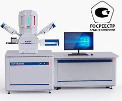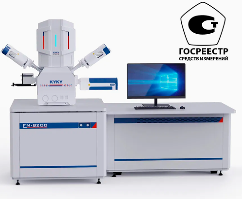
Current KYKY field-emission SEM with stage deceleration, low-aberration objective and Inlens detection. Manufacturer specifications list 0.8 nm SE resolution at 15 kV and 1.5 nm at 1 kV.
Learn More
Description
KYKY EM-8200 Ultra-High-Resolution Field-Emission SEM
The EM-8200 is designed for low-voltage, high-resolution imaging in semiconductor, energy-materials and advanced research applications. It combines stage deceleration, a new low-aberration objective and a low-noise Inlens detector.
| SE resolution | 0.8 nm at 15 kV; 1.5 nm at 1 kV |
|---|---|
| Magnification | 1×–3,000,000×; optical 1×–100× |
| Electron source | Schottky field-emission gun |
| Accelerating voltage | 0.2–30 kV |
| Detectors listed by KYKY | High-vacuum SE, retractable four-segment semiconductor BSE, chamber infrared camera and Inlens |
| Stage | Five-axis motorized large-specimen stage |
| Options | EDS, EBSD, STEM, CL, load lock, heating, cooling and tensile stages |
Confirm installed detectors, analytical ports, stage envelope, site preparation, chilled water or other utilities, vibration and field limits, software licenses and the exact acceptance test.