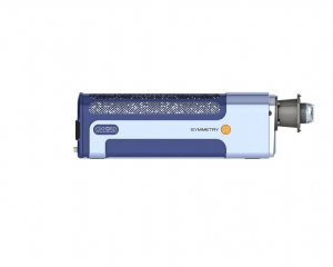
CMOS electron backscatter diffraction system for crystallographic orientation, phase and strain analysis in compatible SEMs. The current C-Nano+ specification lists more than 600 indexed patterns per second and full 1244 × 1024-pixel patterns.
Description
Oxford Instruments C-Nano+ EBSD System
C-Nano+ acquires electron backscatter diffraction patterns for orientation mapping, phase discrimination, grain-boundary analysis and strain-sensitive studies. It can be integrated with Oxford Instruments EDS through the AZtec platform.
| Maximum guaranteed indexing speed | 600 patterns/s at 3 nA |
|---|---|
| Pattern resolution at maximum speed | 311 × 256 pixels |
| Full pattern resolution | 1244 × 1024 pixels |
| Angular precision stated by the manufacturer | Better than 0.05° |
| Detector interface | Lens-free fibre optics with bellows SEM interface |
| Protection | Proximity sensor for collision avoidance |
| Options | Five integrated forescatter detectors and EDS integration |
The former page referred to an earlier C-Nano at 400 frames/s. This revision uses the current C-Nano+ public specification. Confirm SEM chamber geometry, specimen tilt and working distance, beam-current capability, stage repeatability, software modules, phase database and installation clearance.